Amateur Extra / Topics
E7 Practical Circuits
E7 Practical Circuits (Amateur Extra questions)99 questions in 8 groups. The exam asks 8 questions from this topic, one from each group.
E7A Digital circuits: digital circuit principles and logic circuits; classes of logic elements; positive and negative logic; frequency dividers; truth tables
E7A01
Which circuit is bistable?
- A. An AND gate
- B. An OR gate
- C. A flip-flop
- D. A bipolar amplifier
Show answer
C. A flip-flop
A bistable circuit has two stable states and stays in either one until a trigger switches it to the other. A flip-flop is such a circuit: it holds a 1 or a 0 indefinitely, which is why it can store one bit of data.
- A. An AND gate is a combinational circuit with no memory; its output follows its present inputs and it has no state of its own to hold.
- B. An OR gate is also combinational: its output depends only on its present inputs, so it has no stable states to switch between.
- D. A bipolar amplifier is a linear amplifier built with bipolar transistors; its output follows the input signal instead of latching into one of two states.
E7A02
What is the function of a decade counter?
- A. It produces one output pulse for every 10 input pulses
- B. It decodes a decimal number for display on a seven-segment LED display
- C. It produces 10 output pulses for every input pulse
- D. It decodes a binary number for display on a seven-segment LED display
Show answer
A. It produces one output pulse for every 10 input pulses
A decade counter counts input pulses from 0 to 9 and then starts over, producing one output pulse for every 10 input pulses. Used this way it divides a frequency by 10, for example turning a 1 MHz clock into 100 kHz.
- B. Converting a decimal value for a seven-segment display is the job of a display decoder or driver, not a counter.
- C. Producing 10 output pulses for each input pulse would multiply the frequency by 10; a decade counter divides it by 10.
- D. Driving a seven-segment display from a binary number is done by a decoder, such as a BCD-to-seven-segment decoder, not by the counter itself.
E7A03
Which of the following can divide the frequency of a pulse train by 2?
- A. An XOR gate
- B. A flip-flop
- C. An OR gate
- D. A multiplexer
Show answer
B. A flip-flop
A flip-flop wired to toggle changes state once on each input pulse, so two input pulses produce one complete output cycle. The output frequency is half the input frequency, which makes the flip-flop a divide-by-2 circuit.
- A. An XOR gate is combinational: its output depends only on its present inputs, so it cannot count pulses or divide a frequency.
- C. An OR gate has no memory of earlier pulses, so it cannot produce one output cycle for every two input cycles.
- D. A multiplexer selects one of several inputs to pass to its output; it does not divide frequency.
E7A04
How many flip-flops are required to divide a signal frequency by 16?
- A. 4
- B. 6
- C. 8
- D. 16
Show answer
A. 4
Each flip-flop in a chain divides the frequency by 2, so the total division is 2 multiplied by itself once for each flip-flop. Dividing by 16 takes 2 x 2 x 2 x 2 = 16, which is 4 flip-flops.
- B. Six flip-flops divide by 2 x 2 x 2 x 2 x 2 x 2 = 64, not 16.
- C. Eight flip-flops divide by 256 (2 multiplied by itself 8 times), far more than 16.
- D. Sixteen flip-flops would divide by 65,536; 16 is the division ratio, while the number of flip-flops is the power of 2 that produces it, which is 4.
E7A05
Which of the following circuits continuously alternates between two states without an external clock signal?
- A. Monostable multivibrator
- B. J-K flip-flop
- C. T flip-flop
- D. Astable multivibrator
Show answer
D. Astable multivibrator
An astable multivibrator has no stable state, so it switches back and forth between its two states on its own at a rate set by its timing components. It is a free-running oscillator that produces a square wave without any clock or trigger.
- A. A monostable multivibrator has one stable state; it leaves that state only when triggered and returns after a set time, so it does not alternate on its own.
- B. A J-K flip-flop is bistable: it changes state only when clocked, so it needs an external clock to alternate.
- C. A T (toggle) flip-flop changes state once per clock pulse, so it cannot alternate without an external clock signal.
E7A06
What is a characteristic of a monostable multivibrator?
- A. It switches temporarily to an alternate state for a set time
- B. It produces a continuous square wave
- C. It stores one bit of data
- D. It maintains a constant output voltage, regardless of variations in the input voltage
Show answer
A. It switches temporarily to an alternate state for a set time
A monostable multivibrator, or one-shot, has one stable state. A trigger switches it into its other state for a time set by its timing components (often a resistor and capacitor), and then it returns to the stable state on its own.
- B. A continuous square wave comes from an astable multivibrator, which has no stable state.
- C. Storing one bit of data is the role of a bistable circuit, the flip-flop, which stays in either state until switched.
- D. Holding the output voltage constant despite input variations describes a voltage regulator, not a multivibrator.
E7A07
What logical operation does a NAND gate perform?
- A. It produces a 0 at its output only if all inputs are 0
- B. It produces a 1 at its output only if all inputs are 1
- C. It produces a 0 at its output if some but not all inputs are 1
- D. It produces a 0 at its output only if all inputs are 1
Show answer
D. It produces a 0 at its output only if all inputs are 1
A NAND gate is an AND gate followed by an inverter. An AND gate outputs 1 only when all inputs are 1, so a NAND gate outputs 0 only when all inputs are 1 and outputs 1 for every other input combination.
- A. An output of 0 only when all inputs are 0 describes an OR gate.
- B. An output of 1 only when all inputs are 1 describes an AND gate, the opposite of NAND.
- C. For a two-input gate, an output of 0 when some but not all inputs are 1 describes an exclusive NOR gate, which outputs 0 when its inputs differ.
E7A08
What logical operation does an OR gate perform?
- A. It produces a 1 at its output if any input is 1
- B. It produces a 0 at its output if all inputs are 1
- C. It produces a 0 at its output if some but not all inputs are 1
- D. It produces a 1 at its output if all inputs are 0
Show answer
A. It produces a 1 at its output if any input is 1
An OR gate outputs 1 if any one or more of its inputs is 1. Its output is 0 only when all of its inputs are 0.
- B. An output of 0 when all inputs are 1 is NAND behavior; an OR gate outputs 1 in that case.
- C. An output of 0 when some but not all inputs are 1 describes a two-input exclusive NOR gate; an OR gate outputs 1 whenever any input is 1.
- D. An output of 1 when all inputs are 0 is NOR behavior; an OR gate outputs 0 in that case.
E7A09
What logical operation is performed by a two-input exclusive NOR gate?
- A. It produces a 0 at its output only if all inputs are 0
- B. It produces a 1 at its output only if all inputs are 1
- C. It produces a 0 at its output if one and only one of its inputs is 1
- D. It produces a 1 at its output if one and only one input is 1
Show answer
C. It produces a 0 at its output if one and only one of its inputs is 1
A two-input exclusive NOR (XNOR) gate outputs 1 when its inputs are the same (both 0 or both 1) and 0 when they differ. So it produces a 0 when one and only one input is 1; it is the inverse of an exclusive OR gate.
- A. An output of 0 only when all inputs are 0 is OR gate behavior.
- B. An output of 1 only when all inputs are 1 is AND gate behavior; an XNOR gate also outputs 1 when both inputs are 0.
- D. An output of 1 when one and only one input is 1 is the exclusive OR (XOR) function, the inverse of XNOR.
E7A10
What is a truth table?
- A. A list of inputs and corresponding outputs for an op-amp
- B. A list of inputs and corresponding outputs for a digital device
- C. A diagram showing logic states when the digital gate output is true
- D. A table of logic symbols that indicate the logic states of an op-amp
Show answer
B. A list of inputs and corresponding outputs for a digital device
A truth table lists every combination of inputs to a digital device, such as a logic gate, alongside the output each combination produces. It fully describes the device's logic function.
- A. An op-amp is an analog device with continuously varying inputs and outputs, so its behavior is not described by a table of 1s and 0s.
- C. A truth table is a table, not a diagram, and it lists the output for every input combination, whether that output is true or false.
- D. A truth table lists input and output states for a digital device; it is not a table of symbols, and op-amps are analog devices.
E7A11
What does “positive logic” mean in reference to logic devices?
- A. The logic devices have high noise immunity
- B. High voltage represents a 1, low voltage a 0
- C. The logic circuit is in the “true” condition
- D. 1s and 0s are defined as different positive voltage levels
Show answer
B. High voltage represents a 1, low voltage a 0
Positive logic is the convention that the higher voltage level represents a 1 (true) and the lower voltage level represents a 0 (false). Negative logic reverses this, with the lower voltage representing 1.
- A. Noise immunity is a property of a logic family's circuit design, not of the positive or negative logic convention.
- C. Positive logic is a convention for which voltage level means 1; it does not describe whether a circuit is in its true condition.
- D. Both logic levels can be positive voltages under either convention; what defines positive logic is that the higher of the two represents 1.
E7B Amplifiers: class of operation; vacuum tube and solid-state circuits; distortion and intermodulation; spurious and parasitic suppression; switching-type amplifiers
E7B01
For what portion of the signal cycle does each active element in a push-pull, Class AB amplifier conduct?
- A. More than 180 degrees but less than 360 degrees
- B. Exactly 180 degrees
- C. The entire cycle
- D. Less than 180 degrees
Show answer
A. More than 180 degrees but less than 360 degrees
In a Class AB push-pull amplifier, each device is biased slightly on, so it conducts for more than half the cycle (over 180 degrees) but less than the full cycle (360 degrees). The overlap reduces the crossover distortion of Class B while keeping better efficiency than Class A.
- B. Conduction for exactly 180 degrees defines Class B operation.
- C. Conduction for the entire cycle (360 degrees) defines Class A operation.
- D. Conduction for less than 180 degrees defines Class C operation.
E7B02
What is a Class D amplifier?
- A. An amplifier that uses switching technology to achieve high efficiency
- B. A low power amplifier that uses a differential amplifier for improved linearity
- C. An amplifier that uses drift-mode FETs for high efficiency
- D. An amplifier biased to be relatively free from distortion
Show answer
A. An amplifier that uses switching technology to achieve high efficiency
A Class D amplifier operates its active devices as switches that are either fully on or fully off, rather than in their linear region. Because a switch dissipates little power in either state, Class D amplifiers achieve high efficiency.
- B. Class D is defined by switching operation, not by a low-power differential stage; differential amplifiers are a linear building block used in many amplifier classes.
- C. Class D does not depend on a special type of FET; its efficiency comes from switching the device fully on and off.
- D. An amplifier biased to be relatively free from distortion describes Class A, which conducts over the whole cycle at low efficiency.
E7B03
What circuit is required at the output of an RF switching amplifier?
- A. A filter to remove harmonic content
- B. A high-pass filter to compensate for low gain at low frequencies
- C. A matched load resistor to prevent damage by switching transients
- D. A temperature compensating load resistor to improve linearity
Show answer
A. A filter to remove harmonic content
An RF switching amplifier produces a square-wave-like output that is rich in harmonics of the operating frequency. A filter at the output removes those harmonics so that only the desired signal reaches the antenna.
- B. The unwanted output of a switching amplifier is harmonics above the operating frequency; a high-pass filter would pass them rather than remove them.
- C. A load resistor would waste the power the amplifier is meant to deliver; what the output requires is filtering of the harmonic content.
- D. A temperature-compensating load resistor would waste output power and does not remove harmonics, which is what the output circuit must do.
E7B04
What is the operating point of a Class A common emitter amplifier?
- A. Approximately halfway between saturation and cutoff
- B. Approximately halfway between the emitter voltage and the base voltage
- C. At a point where the bias resistor equals the load resistor
- D. At a point where the load line intersects the zero bias current curve
Show answer
A. Approximately halfway between saturation and cutoff
A Class A amplifier must conduct over the entire input cycle, so its operating (quiescent) point is set near the middle of the load line, about halfway between saturation and cutoff. This allows the largest symmetrical output swing without clipping either peak.
- B. The base-emitter voltage of a silicon transistor is only about 0.6 to 0.7 volts; the Class A operating point is set along the load line between saturation and cutoff, not between the emitter and base voltages.
- C. There is no rule that the bias resistor equal the load resistor; the operating point is set by the bias current relative to the load line.
- D. The point where the load line meets the zero-bias-current curve is cutoff, which suits Class B or C operation, not Class A.
E7B05
What can be done to prevent unwanted oscillations in an RF power amplifier?
- A. Tune the stage for minimum loading
- B. Tune both the input and output for maximum power
- C. Install parasitic suppressors and/or neutralize the stage
- D. Use a phase inverter in the output filter
Show answer
C. Install parasitic suppressors and/or neutralize the stage
Unwanted oscillations in an RF power amplifier come from feedback paths, such as the device's internal capacitance or parasitic resonances in its leads. Parasitic suppressors (typically a small coil in parallel with a low-value resistor) damp VHF parasitic oscillations, and neutralization feeds back a signal of opposite phase to cancel the feedback that causes self-oscillation.
- A. Tuning for minimum loading leaves the stage lightly loaded, which raises its gain and makes instability more likely, not less.
- B. Tuning for maximum power adjusts the output at the operating frequency but does not remove the feedback that causes oscillation.
- D. A phase inverter is not part of an output filter, and it would not cancel the feedback paths that cause parasitic oscillation.
E7B06
What is a characteristic of a grounded-grid amplifier?
- A. High power gain
- B. Low input impedance
- C. High electrostatic damage protection
- D. Low bandwidth
Show answer
B. Low input impedance
In a grounded-grid amplifier the grid is at RF ground and the drive signal is applied to the cathode, which presents a low input impedance. That makes the stage easy to drive from a transceiver, and the grounded grid shields the input from the output, giving good stability.
- A. Grounded-grid amplifiers have modest power gain, partly because some of the drive power passes through to the output; high power gain is not their characteristic.
- C. Protection from electrostatic damage is not a characteristic of the grounded-grid configuration.
- D. Grounded-grid amplifiers are known for wide bandwidth and stability, not low bandwidth.
E7B07
Which of the following is the likely result of using a Class C amplifier to amplify a single-sideband phone signal?
- A. Reduced intermodulation products
- B. Increased overall intelligibility
- C. Reduced third-order intermodulation
- D. Signal distortion and excessive bandwidth
Show answer
D. Signal distortion and excessive bandwidth
A Class C amplifier conducts for less than half the cycle, so its output does not track the amplitude of its input. An SSB signal's amplitude varies with the voice, so a Class C stage distorts it badly and generates intermodulation products that spread the signal over excessive bandwidth.
- A. A nonlinear Class C stage increases intermodulation products; it does not reduce them.
- B. The severe amplitude distortion of a Class C stage makes an SSB signal less intelligible, not more.
- C. Third-order intermodulation increases in a nonlinear amplifier, and Class C is highly nonlinear, so it makes these products worse.
E7B08
Why are switching amplifiers more efficient than linear amplifiers?
- A. Switching amplifiers operate at higher voltages
- B. The switching device is at saturation or cutoff most of the time
- C. Linear amplifiers have high gain resulting in higher harmonic content
- D. Switching amplifiers use push-pull circuits
Show answer
B. The switching device is at saturation or cutoff most of the time
A device dissipates power equal to the voltage across it times the current through it. In a switching amplifier the device is either saturated (high current, almost no voltage) or cut off (voltage, but almost no current), so that product stays small most of the time and little power is lost as heat.
- A. Operating voltage does not set efficiency; the low loss comes from the device being fully on or fully off.
- C. Harmonic content does not explain the efficiency difference; switching amplifiers in fact produce more harmonics and need output filtering.
- D. Push-pull circuits are used in both linear and switching amplifiers, so push-pull operation does not explain the efficiency difference.
E7B09
What is characteristic of an emitter follower (or common collector) amplifier?
- A. Low input impedance and phase inversion from input to output
- B. Differential inputs and single output
- C. Acts as an OR circuit if one input is grounded
- D. Input and output signals in-phase
Show answer
D. Input and output signals in-phase
In an emitter follower (common collector), the output is taken from the emitter, which follows the base voltage about 0.6 to 0.7 volts below it. The output is in phase with the input and the voltage gain is slightly less than 1, with high input impedance and low output impedance.
- A. An emitter follower has high input impedance and no phase inversion; phase inversion is characteristic of the common-emitter amplifier.
- B. Differential inputs with a single output describes a differential amplifier, such as the input stage of an op-amp.
- C. An emitter follower is a single-input linear amplifier, not a logic gate.
E7B10
In Figure E7-1, what is the purpose of R1 and R2?
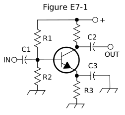
Figure E7-1 - A. Load resistors
- B. Voltage divider bias
- C. Self bias
- D. Feedback
Show answer
B. Voltage divider bias
In Figure E7-1, R1 runs from the positive supply to the transistor's base and R2 runs from the base to ground. Together they form a voltage divider that holds the base at a fixed fraction of the supply voltage, setting the transistor's DC operating point.
- A. The load resistor is the unlabeled resistor between the collector and the positive supply, where the output is taken; R1 and R2 connect to the base.
- C. Self bias in this circuit comes from emitter resistor R3, not from R1 and R2.
- D. R1 and R2 do not connect the output back to the input; they divide the supply voltage to bias the base.
E7B11
In Figure E7-1, what is the purpose of R3?
Figure E7-1 - A. Fixed bias
- B. Emitter bypass
- C. Output load resistor
- D. Self bias
Show answer
D. Self bias
R3 is in series with the emitter. If collector current rises, the voltage across R3 rises and reduces the base-emitter voltage, which pulls the current back down. This self bias stabilizes the DC operating point against changes in temperature and transistor gain.
- A. Fixed bias sets the base current with no correction from the transistor's own current; R3 does the opposite, adjusting the bias automatically as emitter current changes.
- B. The emitter bypass is capacitor C3, connected across R3 to place the emitter at AC ground; R3 is the resistor that sets the DC bias.
- C. The output load resistor is the unlabeled resistor between the collector and the positive supply, not R3 in the emitter lead.
E7B12
What type of amplifier circuit is shown in Figure E7-1?
Figure E7-1 - A. Common base
- B. Common collector
- C. Common emitter
- D. Emitter follower
Show answer
C. Common emitter
In Figure E7-1 the input is coupled to the base through C1, the output is taken from the collector through C2, and the emitter is held at AC ground by bypass capacitor C3. With the emitter common to both input and output, this is a common-emitter amplifier.
- A. A common-base amplifier takes its input at the emitter with the base at AC ground; here the input goes to the base.
- B. A common-collector amplifier takes its output from the emitter; here the output comes from the collector.
- D. An emitter follower is another name for a common-collector amplifier, which takes its output from the emitter, not the collector.
E7C Filters and matching networks: types of networks; types of filters; filter applications; filter characteristics; impedance matching
E7C01
How are the capacitors and inductors of a low-pass filter Pi-network arranged between the network’s input and output?
- A. Two inductors are in series between the input and output, and a capacitor is connected between the two inductors and ground
- B. Two capacitors are in series between the input and output, and an inductor is connected between the two capacitors and ground
- C. An inductor is connected between the input and ground, another inductor is connected between the output and ground, and a capacitor is connected between the input and output
- D. A capacitor is connected between the input and ground, another capacitor is connected between the output and ground, and an inductor is connected between the input and output
Show answer
D. A capacitor is connected between the input and ground, another capacitor is connected between the output and ground, and an inductor is connected between the input and output
A Pi-network is named for its resemblance to the Greek letter pi: two shunt elements to ground joined by one series element. In the low-pass version, a capacitor goes from the input to ground, another from the output to ground, and an inductor connects input to output, so high frequencies are blocked by the inductor and shunted to ground by the capacitors.
- A. Two series inductors with a shunt capacitor between them form a low-pass T-network, not a Pi-network.
- B. Two series capacitors with a shunt inductor between them form a high-pass T-network.
- C. Shunt inductors with a series capacitor do form a Pi-network, but a high-pass one, since the capacitor passes high frequencies and the inductors shunt low frequencies to ground.
E7C02
What is the frequency response of a T-network with series capacitors and a shunt inductor?
- A. Low-pass
- B. High-pass
- C. Band-pass
- D. Notch
Show answer
B. High-pass
A series capacitor passes high frequencies and blocks low ones, while a shunt inductor to ground diverts low frequencies away from the output. A T-network with series capacitors and a shunt inductor therefore passes high frequencies and attenuates low ones, a high-pass response.
- A. A low-pass T-network uses series inductors and a shunt capacitor, the opposite arrangement.
- C. A band-pass response passes a range between two cutoff frequencies; this network has a single cutoff below which it attenuates.
- D. A notch response needs a resonant trap that rejects a narrow range of frequencies; series capacitors with a shunt inductor give a single high-pass cutoff.
E7C03
What is the purpose of adding an inductor to a Pi-network to create a Pi-L-network?
- A. Greater harmonic suppression
- B. Higher efficiency
- C. To eliminate one capacitor
- D. Greater transformation range
Show answer
A. Greater harmonic suppression
A Pi-L-network is a Pi-network followed by an additional series inductor at the output. The extra low-pass section attenuates harmonics further than a Pi-network alone, which is why it is used at the output of transmitters and amplifiers.
- B. The added inductor does not raise efficiency; any added component brings at least a small loss.
- C. The Pi-L-network adds an inductor to a Pi-network; it does not remove a capacitor.
- D. The purpose of the added output inductor is additional harmonic attenuation, not a larger impedance transformation range.
E7C04
How does an impedance-matching circuit transform a complex impedance to a resistive impedance?
- A. It introduces negative resistance to cancel the resistive part of impedance
- B. It introduces transconductance to cancel the reactive part of impedance
- C. It cancels the reactive part of the impedance and changes the resistive part to the desired value
- D. Reactive currents are dissipated in matched resistances
Show answer
C. It cancels the reactive part of the impedance and changes the resistive part to the desired value
An impedance-matching network adds reactance of the opposite sign to cancel the reactive part of the load (capacitive reactance to cancel inductive reactance, for example) and transforms the remaining resistance to the desired value, such as 50 ohms. Ideally it does this with reactive components only, so no power is lost.
- A. A matching network does not cancel the resistive part; it keeps the resistance and transforms it to the desired value, and it uses no negative resistance.
- B. Transconductance is a property of active devices such as transistors; a matching network cancels reactance with opposite reactance.
- D. An ideal matching network dissipates nothing; it cancels reactance with opposite reactance rather than burning off reactive currents in resistors.
E7C05
Which filter type has ripple in the passband and a sharp cutoff?
- A. A Butterworth filter
- B. An active LC filter
- C. A passive op-amp filter
- D. A Chebyshev filter
Show answer
D. A Chebyshev filter
A Chebyshev filter allows a controlled amount of ripple in its passband in exchange for a steeper rolloff beyond cutoff than a Butterworth filter of the same order. Allowing more ripple gives a sharper cutoff.
- A. A Butterworth filter has a flat passband with no ripple and a more gradual cutoff.
- B. An active filter uses amplifying devices, and an LC filter can be designed for any response type; neither term identifies the passband ripple and sharp cutoff of a Chebyshev design.
- C. An op-amp filter is by definition an active filter, so a passive op-amp filter is a contradiction, not a filter response type.
E7C06
What are the characteristics of an elliptical filter?
- A. Gradual passband rolloff with minimal stop-band ripple
- B. Extremely flat response over its pass band with gradually rounded stop-band corners
- C. Extremely sharp cutoff with one or more notches in the stop band
- D. Gradual passband rolloff with extreme stop-band ripple
Show answer
C. Extremely sharp cutoff with one or more notches in the stop band
An elliptical (Cauer) filter places one or more notches in the stop band close to the cutoff frequency. This gives an extremely sharp transition from passband to stop band, at the cost of ripple in both the passband and the stop band.
- A. Gradual rolloff with little stop-band ripple is closer to a Butterworth or Bessel filter; an elliptical filter has a very sharp cutoff.
- B. An extremely flat passband with gradual rolloff describes a Butterworth filter.
- D. An elliptical filter does have stop-band ripple from its notches, but its rolloff is very sharp, not gradual.
E7C07
Which describes a Pi-L network?
- A. A Phase Inverter Load network
- B. A Pi-network with an additional output series inductor
- C. A network with only three discrete parts
- D. A matching network in which all components are isolated from ground
Show answer
B. A Pi-network with an additional output series inductor
A Pi-L network is a Pi-network (shunt capacitor, series inductor, shunt capacitor) with one more inductor in series at the output, forming an L section. It is common as an amplifier output network because of its added harmonic suppression.
- A. Pi refers to the circuit's resemblance to the Greek letter pi; it does not stand for phase inverter.
- C. A basic Pi-network has three parts; the Pi-L network adds a fourth, the output series inductor.
- D. A Pi-L network has shunt capacitors connected to ground, so its components are not all isolated from ground.
E7C08
Which of the following is most frequently used as a band-pass or notch filter in VHF and UHF transceivers?
- A. A Sallen-Key filter
- B. A helical filter
- C. A swinging choke filter
- D. A finite impulse response filter
Show answer
B. A helical filter
A helical filter uses coil-shaped resonators inside shielded cans, giving high Q in a compact size at VHF and UHF. VHF and UHF equipment commonly uses helical filters as band-pass or notch filters.
- A. A Sallen-Key filter is an active RC filter built around an op-amp, used at audio and low frequencies, not as an RF filter at VHF and UHF.
- C. A swinging choke is an inductor in power supply filters whose inductance varies with current; it is not an RF filter.
- D. A finite impulse response filter is a digital filter that runs on sampled data in DSP; it is not the usual band-pass or notch filter in a VHF or UHF RF stage.
E7C09
What is a crystal lattice filter?
- A. A power supply filter made with interlaced quartz crystals
- B. An audio filter made with four quartz crystals that resonate at 1 kHz intervals
- C. A filter using lattice-shaped quartz crystals for high-Q performance
- D. A filter for low-level signals made using quartz crystals
Show answer
D. A filter for low-level signals made using quartz crystals
A crystal lattice filter uses quartz crystals on slightly different frequencies connected in a lattice (bridge) arrangement. The crystals' high Q gives a narrow, steep-sided passband, but they cannot handle much power, so these filters are used with low-level signals, such as in receiver IF stages.
- A. Quartz crystals cannot carry power supply currents; power supplies are filtered with capacitors and inductors.
- B. Crystal lattice filters work at radio frequencies, usually in IF stages; they are not audio filters with crystals spaced 1 kHz apart.
- C. Lattice refers to how the crystals are connected in the circuit, not to the shape of the crystals.
E7C10
Which of the following filters is used in a 2-meter band repeater duplexer?
- A. A crystal filter
- B. A cavity filter
- C. A DSP filter
- D. An L-C filter
Show answer
B. A cavity filter
A repeater duplexer lets the transmitter and receiver share one antenna while operating only 600 kHz apart on 2 meters. That requires very high Q filters that can also handle transmitter power, which is what resonant cavity filters provide.
- A. Crystal filters handle only low-level signals and cannot pass transmitter power to the antenna.
- C. A DSP filter works on digitized signals inside a radio; it cannot filter the RF power flowing between the transmitter, receiver, and antenna.
- D. Ordinary L-C filters do not have enough Q to separate signals only 600 kHz apart at 2 meters with the deep rejection a duplexer needs.
E7C11
Which of the following measures a filter’s ability to reject signals in adjacent channels?
- A. Passband ripple
- B. Phase response
- C. Shape factor
- D. Noise factor
Show answer
C. Shape factor
Shape factor is the ratio of a filter's bandwidth at a high attenuation level to its bandwidth at a low attenuation level, for example the 60 dB bandwidth divided by the 6 dB bandwidth. A shape factor closer to 1 means steeper skirts and better rejection of signals in adjacent channels.
- A. Passband ripple is the variation in response within the passband, not the rejection of signals outside it.
- B. Phase response describes how a filter shifts the phase of signals at different frequencies, not how well it rejects adjacent signals.
- D. Noise factor measures how much noise a device adds to a signal, not its selectivity.
E7D Power supplies and voltage regulators; solar array charge controllers
E7D01
How does a linear electronic voltage regulator work?
- A. It has a ramp voltage as its output
- B. It eliminates the need for a pass transistor
- C. The control element duty cycle is proportional to the line or load conditions
- D. The conduction of a control element is varied to maintain a constant output voltage
Show answer
D. The conduction of a control element is varied to maintain a constant output voltage
A linear regulator uses a control element, usually a transistor, operating in its linear region. Its conduction is varied continuously, like a variable resistor, to drop whatever voltage is needed to keep the output constant as the input voltage and load current change.
- A. A regulator holds its output at a steady DC voltage; a ramp output describes a sweep or sawtooth generator.
- B. A series linear regulator relies on a pass transistor as its control element; it does not eliminate it.
- C. Varying the duty cycle of a control element describes a switching regulator, not a linear one.
E7D02
How does a switchmode voltage regulator work?
- A. By alternating the output between positive and negative voltages
- B. By varying the duty cycle of pulses input to a filter
- C. By varying the conductivity of a pass element
- D. By switching between two Zener diode reference voltages
Show answer
B. By varying the duty cycle of pulses input to a filter
A switchmode regulator turns a transistor fully on and off at high frequency, producing pulses that an inductor and capacitor filter smooth into DC. The control circuit varies the duty cycle (the fraction of each period the switch is on) to hold the output voltage constant.
- A. Alternating between positive and negative voltages produces AC, which is what an inverter does, not how a regulator holds a DC voltage.
- C. Varying the conductivity of a pass element describes a linear regulator.
- D. A switchmode regulator compares its output against a single stable reference; it does not switch between two Zener references.
E7D03
What device is used as a stable voltage reference?
- A. A Zener diode
- B. A digital-to-analog converter
- C. An SCR
- D. An analog-to-digital converter
Show answer
A. A Zener diode
A Zener diode operated in reverse breakdown holds a nearly constant voltage across itself over a wide range of current. That makes it a common voltage reference in regulators and other circuits.
- B. A digital-to-analog converter needs a stable voltage reference to work accurately; it is not used as one.
- C. An SCR is a latching switch, used for example in crowbar overvoltage protection, not a voltage reference.
- D. An analog-to-digital converter measures voltages against a reference; it does not provide one.
E7D04
Which of the following describes a three-terminal voltage regulator?
- A. A series current source
- B. A series regulator
- C. A shunt regulator
- D. A shunt current source
Show answer
B. A series regulator
A three-terminal voltage regulator IC, such as a 7805 or LM317, has input, output, and ground (or adjust) terminals. Its pass transistor is in series between input and output, so it is a series regulator.
- A. A three-terminal regulator holds a constant output voltage, not a constant current.
- C. A shunt regulator connects in parallel with the load; a three-terminal regulator places its control element in series.
- D. A shunt current source neither regulates voltage nor matches the series arrangement of a three-terminal regulator.
E7D05
Which of the following types of linear voltage regulator operates by loading the unregulated voltage source?
- A. A constant current source
- B. A series regulator
- C. A shunt current source
- D. A shunt regulator
Show answer
D. A shunt regulator
A shunt regulator connects in parallel with the load and draws a varying current from the source through a series resistor. By loading the source more or less heavily, it keeps the output voltage constant; a Zener diode with a series resistor is the basic example.
- A. A constant current source holds current, not voltage, constant, so it is not a type of linear voltage regulator.
- B. A series regulator varies the conduction of an element in series with the load rather than loading the source in parallel.
- C. A shunt current source is not a voltage regulator; the regulator that works by loading the source is the shunt regulator.
E7D06
What is the purpose of Q1 in the circuit shown in Figure E7-2?
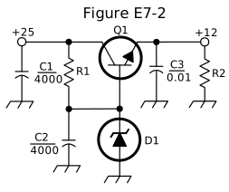
Figure E7-2 - A. It provides negative feedback to improve regulation
- B. It provides a constant load for the voltage source
- C. It controls the current to keep the output voltage constant
- D. It provides regulation by switching or “chopping” the input DC voltage
Show answer
C. It controls the current to keep the output voltage constant
Q1 is the series pass transistor: its collector connects to the unregulated +25 volt input and its emitter supplies the +12 volt output. Zener diode D1 holds Q1's base at a fixed voltage, and because the emitter stays about 0.6 to 0.7 volts below the base, Q1 adjusts the current it passes to keep the output voltage constant as the load changes.
- A. The circuit has no separate feedback network or error amplifier; regulation comes from Q1 following the fixed base voltage set by D1.
- B. Providing a constant load for the source describes a shunt regulator; Q1 is in series with the load.
- D. Nothing in this circuit switches or chops the input; Q1 operates in its linear region, and there is no inductor or switching control.
E7D07
What is the purpose of C2 in the circuit shown in Figure E7-2?
Figure E7-2 - A. It bypasses rectifier output ripple around D1
- B. It is a brute force filter for the output
- C. To prevent self-oscillation
- D. To provide fixed DC bias for Q1
Show answer
A. It bypasses rectifier output ripple around D1
C2 is connected across Zener diode D1, from Q1's base to ground. It bypasses rectifier ripple and noise arriving through R1, keeping the reference voltage at Q1's base smooth so the regulated output is smooth too.
- B. C2 sits at the base reference point, not in the output path; C1 is the large input filter capacitor and C3 is at the output.
- C. C2 is placed across the Zener reference to filter ripple, not to suppress oscillation.
- D. A capacitor passes no DC, so it cannot provide DC bias; Q1's base bias comes from R1 and Zener diode D1.
E7D08
What type of circuit is shown in Figure E7-2?
Figure E7-2 - A. Switching voltage regulator
- B. Common emitter amplifier
- C. Linear voltage regulator
- D. Common base amplifier
Show answer
C. Linear voltage regulator
Figure E7-2 shows a series pass transistor, Q1, whose base is held at a fixed voltage by Zener diode D1, dropping an unregulated +25 volts to a regulated +12 volts. Q1 operates continuously in its linear region, so this is a linear voltage regulator.
- A. A switching regulator needs a switching control circuit and an inductor to filter the pulses; this circuit has neither.
- B. There is no signal input to Q1's base and the output comes from its emitter, so this is not a common emitter amplifier.
- D. A common base amplifier has its input at the emitter and its base at AC ground; Q1 here supplies the output from its emitter as a pass element.
E7D09
How is battery operating time calculated?
- A. Average current divided by capacity in amp-hours
- B. Average current divided by internal resistance
- C. Capacity in amp-hours divided by average current
- D. Internal resistance divided by average current
Show answer
C. Capacity in amp-hours divided by average current
A battery's capacity in amp-hours is the current it can supply multiplied by the hours it can supply it. Dividing capacity by the average current gives the operating time: for example, 20 amp-hours / 4 amps = 5 hours.
- A. Average current divided by capacity is the inverse of the operating time, not the time itself.
- B. Internal resistance affects the voltage drop under load; dividing current by it does not give a time.
- D. Internal resistance divided by current does not produce a time; operating time comes from capacity and current.
E7D10
Why is a switching type power supply less expensive and lighter than an equivalent linear power supply?
- A. The inverter design does not require an output filter circuit
- B. The control circuitry uses less current, therefore smaller heat sinks are required
- C. The high frequency inverter design uses much smaller transformers and filter components for an equivalent power output
- D. It recovers power from the unused portion of the AC cycle, thus using fewer components
Show answer
C. The high frequency inverter design uses much smaller transformers and filter components for an equivalent power output
A switching supply converts power at a high frequency, typically tens or hundreds of kilohertz, instead of the 60 Hz power line frequency. The transformer and filter components needed for a given power get smaller as frequency rises, so the supply uses smaller, lighter, less costly parts.
- A. Switching supplies do need output filtering to smooth the high-frequency pulses into DC.
- B. Smaller heat sinks follow from the switching device's efficiency, not from the control circuitry drawing less current, and the main savings are in the transformer and filter.
- D. A switching supply does not recover power from an unused part of the AC cycle; its savings come from operating at high frequency.
E7D11
What is the purpose of an inverter connected to a solar panel output?
- A. Reduce AC ripple on the output
- B. Maintain voltage with varying illumination levels
- C. Prevent discharge when panel is not illuminated
- D. Convert the panel’s output from DC to AC
Show answer
D. Convert the panel’s output from DC to AC
A solar panel produces DC. An inverter converts that DC into AC so it can run AC-powered equipment or feed AC power to the grid.
- A. Reducing ripple is the job of a filter; a solar panel's output is DC, and the inverter creates AC from it.
- B. Holding voltage steady as illumination changes is the job of a charge controller or regulator.
- C. Preventing a battery from discharging back through an unlit panel is done by a blocking diode or the charge controller.
E7D12
What is the dropout voltage of a linear voltage regulator?
- A. Minimum input voltage for rated power dissipation
- B. Maximum output voltage drop when the input voltage is varied over its specified range
- C. Minimum input-to-output voltage required to maintain regulation
- D. Maximum that the output voltage may decrease at rated load
Show answer
C. Minimum input-to-output voltage required to maintain regulation
Dropout voltage is the smallest difference between input and output voltage at which a linear regulator can still hold its output in regulation. For example, a 5-volt regulator with 2 volts of dropout needs at least 7 volts at its input.
- A. Dropout voltage concerns keeping the output in regulation, not reaching rated power dissipation.
- B. The change in output as the input varies over its range is the line regulation specification.
- D. The allowed output decrease at rated load is a load regulation specification.
E7D13
Which of the following calculates power dissipated by a series linear voltage regulator?
- A. Input voltage multiplied by input current
- B. Input voltage divided by output current
- C. Voltage difference from input to output multiplied by output current
- D. Output voltage multiplied by output current
Show answer
C. Voltage difference from input to output multiplied by output current
The series pass element carries the full load current while dropping the difference between input and output voltage, so it dissipates P = (Vin - Vout) x Iout. For example, 15 volts in and 12 volts out at 2 amps gives (15 - 12) x 2 = 6 watts of heat in the regulator.
- A. Input voltage times input current is the total power drawn from the source, which includes the power delivered to the load.
- B. Voltage divided by current is a resistance in ohms, not a power.
- D. Output voltage times output current is the power delivered to the load, not the power lost in the regulator.
E7D14
What is the purpose of connecting equal-value resistors across power supply filter capacitors connected in series?
- A. Equalize the voltage across each capacitor
- B. Discharge the capacitors when voltage is removed
- C. Provide a minimum load on the supply
- D. All these choices are correct
Show answer
D. All these choices are correct
Equal-value resistors across series-connected filter capacitors do three jobs at once: they divide the voltage evenly between the capacitors, bleed off the stored charge when the supply is turned off, and draw a small minimum load current that helps regulation.
- A. Equalizing the voltage is a real purpose, since capacitors with unequal leakage would otherwise share the voltage unevenly, but it is only one of the three.
- B. Discharging the capacitors is a real purpose, since the resistors bleed off dangerous stored charge after power is removed, but it is only one of the three.
- C. Providing a minimum load is a real purpose, since the steady current through the resistors helps regulation, but it is only one of the three.
E7D15
What is the purpose of a step-start circuit in a high-voltage power supply?
- A. To provide a dual-voltage output for reduced power applications
- B. To compensate for variations of the incoming line voltage
- C. To prevent arcing across the input power switch or relay contacts
- D. To allow the filter capacitors to charge gradually
Show answer
D. To allow the filter capacitors to charge gradually
Uncharged filter capacitors look like a short circuit when power is first applied, so a high-voltage supply can draw a large inrush current. A step-start circuit places a resistance in series at turn-on and bypasses it after a short delay, letting the filter capacitors charge gradually and protecting the rectifiers, transformer and fuses.
- A. Step-start does not provide a second output voltage; it only limits current during turn-on.
- B. Compensating for line voltage variations is the job of a voltage regulator, not a turn-on circuit.
- C. Step-start is aimed at the inrush current that charges the filter capacitors, not at contact arcing; any reduced stress on switch contacts is a side effect.
E7E Modulation and demodulation: reactance, phase, and balanced modulators; detectors; mixers
E7E01
Which of the following can be used to generate FM phone signals?
- A. Balanced modulation of the audio amplifier
- B. Reactance modulation of a local oscillator
- C. Reactance modulation of the final amplifier
- D. Balanced modulation of a local oscillator
Show answer
B. Reactance modulation of a local oscillator
FM requires varying the frequency of the oscillator that sets the carrier. A reactance modulator, a circuit that acts as a variable capacitance or inductance controlled by the audio, shifts the oscillator's frequency in step with the audio to produce FM.
- A. Balanced modulation produces a double-sideband suppressed-carrier signal, the first step in making SSB; applied to an audio amplifier it does not vary a carrier's frequency.
- C. The final amplifier does not set the carrier frequency, so varying its reactance does not produce controlled frequency modulation.
- D. Balanced modulation produces sidebands with the carrier suppressed, which is used for SSB, not FM.
E7E02
What is the function of a reactance modulator?
- A. Produce PM or FM signals by varying a resistance
- B. Produce AM signals by varying an inductance
- C. Produce AM signals by varying a resistance
- D. Produce PM or FM signals by varying a capacitance
Show answer
D. Produce PM or FM signals by varying a capacitance
A reactance modulator acts as a variable reactance, usually a capacitance, controlled by the audio signal. Placed in an oscillator's tuned circuit it varies the frequency (FM); acting on a tuned circuit after the oscillator it varies the phase (PM).
- A. A reactance modulator varies reactance, not resistance; varying a resistance would change amplitude rather than frequency or phase.
- B. Varying a reactance changes frequency or phase, producing FM or PM, not AM.
- C. Varying a resistance can change amplitude, but that is not what a reactance modulator does; it varies reactance to produce FM or PM.
E7E03
What is a frequency discriminator?
- A. An FM generator circuit
- B. A circuit for filtering closely adjacent signals
- C. An automatic band-switching circuit
- D. A circuit for detecting FM signals
Show answer
D. A circuit for detecting FM signals
A frequency discriminator converts changes in frequency into changes in voltage. The frequency deviation of an FM signal becomes the recovered audio, so the discriminator is an FM detector.
- A. Generating FM is done by a modulator, such as a reactance modulator acting on an oscillator; a discriminator recovers audio from FM.
- B. Separating closely spaced signals is the job of selective filters, not a discriminator.
- C. Automatic band switching is a control function unrelated to detecting FM.
E7E04
What is one way to produce a single-sideband phone signal?
- A. Use a balanced modulator followed by a filter
- B. Use a reactance modulator followed by a mixer
- C. Use a loop modulator followed by a mixer
- D. Use a product detector with a DSB signal
Show answer
A. Use a balanced modulator followed by a filter
A balanced modulator mixes audio with a carrier and suppresses the carrier, leaving a double-sideband signal. A sharp filter then removes one sideband, leaving single sideband; this is the filter method of SSB generation.
- B. A reactance modulator produces FM or PM, and a mixer only shifts that signal to another frequency.
- C. Mixing only shifts a signal to a new frequency; generating SSB requires suppressing the carrier and removing one sideband, which this arrangement does not do.
- D. A product detector is a receiver circuit that recovers audio from SSB or CW signals; it does not create an SSB signal.
E7E05
What is added to an FM speech channel to boost the higher audio frequencies?
- A. A de-emphasis network
- B. A harmonic enhancer
- C. A heterodyne enhancer
- D. A pre-emphasis network
Show answer
D. A pre-emphasis network
Pre-emphasis boosts the higher audio frequencies before modulation in an FM transmitter, raising them above the noise that FM reception adds mostly at higher audio frequencies. The receiver applies matching de-emphasis to restore a flat audio response.
- A. De-emphasis is the receiver network that cuts the higher audio frequencies to undo pre-emphasis.
- B. A harmonic enhancer is not a standard part of an FM speech channel; boosting the higher audio frequencies is done by pre-emphasis.
- C. A heterodyne enhancer is not a standard FM circuit; the network that boosts the higher audio frequencies is pre-emphasis.
E7E06
Why is de-emphasis used in FM communications receivers?
- A. For compatibility with transmitters using phase modulation
- B. To reduce impulse noise reception
- C. For higher efficiency
- D. To remove third-order distortion products
Show answer
A. For compatibility with transmitters using phase modulation
Phase modulation inherently produces frequency deviation that increases with audio frequency, which has the same effect as pre-emphasis. A receiver with de-emphasis rolls off the higher audio frequencies, so signals from phase-modulated transmitters (and FM transmitters with pre-emphasis) come out with a flat audio response.
- B. De-emphasis lowers high-frequency hiss when paired with pre-emphasis, but it is not aimed at impulse noise, which an FM receiver's limiter handles.
- C. De-emphasis is an audio filter that shapes frequency response; it does not improve efficiency.
- D. De-emphasis is a frequency-response correction, not a way to remove third-order distortion products.
E7E07
What is meant by the term “baseband” in radio communications?
- A. The lowest frequency band that the transmitter or receiver covers
- B. The frequency range occupied by a message signal prior to modulation
- C. The unmodulated bandwidth of the transmitted signal
- D. The basic oscillator frequency in an FM transmitter that is multiplied to increase the deviation and carrier frequency
Show answer
B. The frequency range occupied by a message signal prior to modulation
Baseband is the frequency range of the message signal itself before it modulates a carrier, such as the audio from about 300 to 3000 Hz in a voice channel. Modulation shifts that baseband information up to the radio frequency.
- A. Baseband refers to the message signal before modulation, not to the lowest band a transmitter or receiver covers.
- C. An unmodulated carrier carries no message; baseband is the frequency range of the message signal itself.
- D. A low-frequency oscillator followed by frequency multipliers describes some FM transmitters, not baseband.
E7E08
What are the principal frequencies that appear at the output of a mixer?
- A. Two and four times the input frequency
- B. The square root of the product of input frequencies
- C. The two input frequencies along with their sum and difference frequencies
- D. 1.414 and 0.707 times the input frequency
Show answer
C. The two input frequencies along with their sum and difference frequencies
A mixer combines two input frequencies in a nonlinear way, so its output contains the two original frequencies plus their sum and their difference. For example, 14 MHz and 9 MHz inputs also produce 23 MHz and 5 MHz, and a filter selects the wanted product.
- A. Two and four times an input frequency are harmonics, the output of a frequency multiplier, not the principal mixer products.
- B. The square root of the product of two frequencies is their geometric mean, which is not a mixer output.
- D. 1.414 and 0.707 are the ratios between the peak and RMS values of a sine wave, not frequencies produced by a mixer.
E7E09
What occurs when the input signal levels to a mixer are too high?
- A. Spurious mixer products are generated
- B. Mixer blanking occurs
- C. Automatic limiting occurs
- D. Excessive AGC voltage levels are generated
Show answer
A. Spurious mixer products are generated
A mixer is meant to produce mainly the sum and difference of its inputs. When input levels are too high the mixer is overdriven, and its nonlinearity creates many additional spurious products, such as intermodulation products, that appear as unwanted signals.
- B. Mixer blanking is not a recognized effect; blanking refers to noise blankers, which silence the receiver during noise pulses.
- C. Limiting is a deliberate function of a limiter stage, as in FM receivers; overdriving a mixer causes distortion and spurious products, not useful limiting.
- D. AGC voltage is derived from signal level in later stages; the characteristic result of overdriving a mixer is spurious products.
E7E10
How does a diode envelope detector function?
- A. By rectification and filtering of RF signals
- B. By breakdown of the Zener voltage
- C. By mixing signals with noise in the transition region of the diode
- D. By sensing the change of reactance in the diode with respect to frequency
Show answer
A. By rectification and filtering of RF signals
A diode envelope detector rectifies the RF signal, passing only one polarity, and a capacitor and resistor then filter out the RF. What remains follows the peaks of the signal, which is the modulation envelope of an AM signal.
- B. Zener breakdown is the reverse-bias effect used for voltage regulation, not detection.
- C. Detection does not rely on mixing signals with noise in the diode; it relies on rectifying the signal.
- D. An envelope detector responds to amplitude, not frequency; responding to frequency changes is the job of FM detectors.
E7E11
Which type of detector is used for demodulating SSB signals?
- A. Discriminator
- B. Phase detector
- C. Product detector
- D. Phase comparator
Show answer
C. Product detector
A product detector mixes the SSB signal with a locally generated carrier from a beat frequency oscillator (BFO), replacing the carrier that was suppressed at the transmitter. The difference product is the recovered audio, which is why product detectors are used for SSB and CW.
- A. A discriminator converts frequency changes to voltage and demodulates FM, not SSB.
- B. A phase detector compares the phase of two signals, as in a phase-locked loop; it is not used to recover SSB audio.
- D. A phase comparator is another name for a phase detector, used in phase-locked loops, not for SSB demodulation.
E7F Software defined radio fundamentals: digital signal processing (DSP) filtering, modulation, and demodulation; analog-digital conversion; digital filters
E7F01
What is meant by “direct sampling” in software defined radios?
- A. Software is converted from source code to object code during operation of the receiver
- B. I and Q signals are generated by digital processing without the use of RF amplification
- C. Incoming RF is digitized by an analog-to-digital converter without being mixed with a local oscillator signal
- D. A switching mixer is used to generate I and Q signals directly from the RF input
Show answer
C. Incoming RF is digitized by an analog-to-digital converter without being mixed with a local oscillator signal
In a direct-sampling SDR, an analog-to-digital converter digitizes the RF signal from the antenna (after filtering, and usually some amplification) without first mixing it with a local oscillator. Tuning, filtering, and demodulation are then all done digitally.
- A. Converting source code to object code is software compilation, unrelated to how a receiver samples RF.
- B. Direct sampling is defined by digitizing RF without analog mixing; it does not mean leaving out RF amplification.
- D. A switching mixer that produces I and Q signals is a quadrature sampling detector, which does mix the RF with a local oscillator before digitizing.
E7F02
What kind of digital signal processing audio filter is used to remove unwanted noise from a received SSB signal?
- A. An adaptive filter
- B. A crystal-lattice filter
- C. A Hilbert-transform filter
- D. A phase-inverting filter
Show answer
A. An adaptive filter
An adaptive filter continually adjusts its coefficients based on the incoming signal. For noise reduction it tracks the predictable, correlated parts of the audio, such as speech, and suppresses random noise, improving a received SSB signal.
- B. A crystal-lattice filter is an analog RF or IF filter made with quartz crystals, not a DSP audio filter.
- C. A Hilbert-transform filter provides a 90-degree phase shift used to generate or demodulate SSB, not to remove noise.
- D. Inverting a signal's phase does not separate noise from speech, so a phase-inverting filter is not a DSP noise-reduction method.
E7F03
What type of digital signal processing filter is used to generate an SSB signal?
- A. An adaptive filter
- B. A notch filter
- C. A Hilbert-transform filter
- D. An elliptical filter
Show answer
C. A Hilbert-transform filter
A Hilbert-transform filter shifts every frequency in the audio by 90 degrees. Combining the shifted and unshifted audio with carriers 90 degrees apart cancels one sideband, which is the phasing method of SSB generation carried out in DSP.
- A. An adaptive filter adjusts itself to the signal and is used for noise reduction or automatic notching, not SSB generation.
- B. A notch filter removes a narrow band of frequencies, such as a heterodyne; it does not generate SSB.
- D. An elliptical filter is a sharp-cutoff filter design; the DSP filter that generates SSB by phasing is the Hilbert transformer.
E7F04
Which method generates an SSB signal using digital signal processing?
- A. Mixing products are converted to voltages and subtracted by adder circuits
- B. A frequency synthesizer removes unwanted sidebands
- C. Varying quartz crystal characteristics are emulated in digital form
- D. Signals are combined in quadrature phase relationship
Show answer
D. Signals are combined in quadrature phase relationship
DSP generates SSB with the phasing method: the audio and the carrier are each split into two paths 90 degrees apart (the I and Q, or in-phase and quadrature, signals), mixed, and combined. One sideband adds and the other cancels, leaving a single sideband.
- A. Converting mixing products to voltages and subtracting them with adder circuits is not a defined SSB method, and it describes analog hardware rather than DSP.
- B. A frequency synthesizer generates frequencies; it does not remove an unwanted sideband.
- C. DSP does not emulate quartz crystals to make SSB; it generates SSB mathematically by combining signals in quadrature.
E7F05
How frequently must an analog signal be sampled to be accurately reproduced?
- A. At least half the rate of the highest frequency component of the signal
- B. At least twice the rate of the highest frequency component of the signal
- C. At the same rate as the highest frequency component of the signal
- D. At four times the rate of the highest frequency component of the signal
Show answer
B. At least twice the rate of the highest frequency component of the signal
The Nyquist sampling theorem says a signal must be sampled at least twice as fast as its highest frequency component to be reproduced without aliasing. For example, audio extending to 3 kHz needs at least 6,000 samples per second.
- A. Sampling at half the highest frequency is far too slow; components above half the sample rate alias into false lower frequencies.
- C. Sampling at the same rate as a frequency captures the same point of each cycle, so that component aliases and appears as a constant (DC) value.
- D. Four times the highest frequency works but is more than required; the minimum is twice the highest frequency.
E7F06
What is the minimum number of bits required to sample a signal with a range of 1 volt at a resolution of 1 millivolt?
- A. 4 bits
- B. 6 bits
- C. 8 bits
- D. 10 bits
Show answer
D. 10 bits
A 1-volt range at 1-millivolt resolution needs 1 V / 1 mV = 1,000 distinct levels. An n-bit converter has 2 to the power n levels: 9 bits give only 512, while 10 bits give 1,024 (about 0.98 mV per step), so 10 bits is the minimum.
- A. 4 bits give only 16 levels, about 62.5 mV per step.
- B. 6 bits give 64 levels, about 15.6 mV per step.
- C. 8 bits give 256 levels, about 3.9 mV per step, still too coarse for 1 mV resolution.
E7F07
What function is performed by a Fast Fourier Transform?
- A. Converting analog signals to digital form
- B. Converting digital signals to analog form
- C. Converting signals from the time domain to the frequency domain
- D. Converting signals from the frequency domain to the time domain
Show answer
C. Converting signals from the time domain to the frequency domain
A Fast Fourier Transform is an efficient algorithm that converts a block of samples in the time domain into its frequency components. SDRs use it, for example, to draw spectrum and waterfall displays.
- A. Converting analog signals to digital form is done by an analog-to-digital converter.
- B. Converting digital signals to analog form is done by a digital-to-analog converter.
- D. Converting from the frequency domain back to the time domain is done by the inverse FFT.
E7F08
What is the function of decimation?
- A. Converting data to binary-coded decimal form
- B. Reducing the effective sample rate by removing samples
- C. Attenuating the signal
- D. Removing unnecessary significant digits
Show answer
B. Reducing the effective sample rate by removing samples
Decimation reduces a signal's sample rate by keeping only some of the samples; keeping every fourth sample, for example, divides the rate by 4. A low-pass filter comes first so the lower rate does not cause aliasing, and the reduced rate lowers the processing load in later stages.
- A. Binary-coded decimal is a way of representing numbers and has nothing to do with decimation.
- C. Attenuation reduces a signal's amplitude; decimation reduces its sample rate.
- D. Removing significant digits is rounding or truncation of numbers, not decimation.
E7F09
Why is an anti-aliasing filter required in a decimator?
- A. It removes high-frequency signal components that would otherwise be reproduced as lower frequency components
- B. It peaks the response of the decimator, improving bandwidth
- C. It removes low-frequency signal components to eliminate the need for DC restoration
- D. It notches out the sampling frequency to avoid sampling errors
Show answer
A. It removes high-frequency signal components that would otherwise be reproduced as lower frequency components
After decimation, the new, lower sample rate can represent only frequencies below half that rate. Any components above that limit would fold back (alias) and appear as false lower-frequency signals, so a low-pass anti-aliasing filter removes them before samples are discarded.
- B. An anti-aliasing filter removes unwanted frequencies; it does not peak the decimator's response or improve bandwidth.
- C. Aliasing comes from high-frequency components, so the filter removes high frequencies, not low ones.
- D. Removing one frequency is not enough; every component above half the new sample rate must be removed to prevent aliasing.
E7F10
What aspect of receiver analog-to-digital conversion determines the maximum receive bandwidth of a direct-sampling software defined radio (SDR)?
- A. Sample rate
- B. Sample width in bits
- C. Integral non-linearity
- D. Differential non-linearity
Show answer
A. Sample rate
By the Nyquist criterion, an analog-to-digital converter can capture a bandwidth of at most half its sample rate. A direct-sampling SDR's sample rate therefore sets the widest bandwidth it can receive; for example, 100 million samples per second covers at most 50 MHz.
- B. Sample width in bits sets resolution and dynamic range, not bandwidth.
- C. Integral non-linearity is a conversion accuracy error that causes distortion; it does not set bandwidth.
- D. Differential non-linearity is an error in the size of individual steps; it affects accuracy, not bandwidth.
E7F11
What sets the minimum detectable signal level for a direct-sampling software defined receiver in the absence of atmospheric or thermal noise?
- A. Sample clock phase noise
- B. Reference voltage level and sample width in bits
- C. Data storage transfer rate
- D. Missing codes and jitter
Show answer
B. Reference voltage level and sample width in bits
The smallest change an analog-to-digital converter can resolve is one step, which equals the reference voltage (its full-scale range) divided by 2 raised to the number of bits. A lower reference voltage or more bits makes each step smaller, so with no external noise those two values set the minimum detectable signal.
- A. Sample clock phase noise degrades the purity of the digitized signal, but it does not set the smallest step the converter can resolve.
- C. Data storage transfer rate limits how fast samples can be moved, not how small a signal can be detected.
- D. Missing codes and jitter are converter imperfections that add errors; the basic limit is the step size set by the reference voltage and bit count.
E7F12
Which of the following is generally true of Finite Impulse Response (FIR) filters?
- A. FIR filters can delay all frequency components of the signal by the same amount
- B. FIR filters are easier to implement for a given set of passband rolloff requirements
- C. FIR filters can respond faster to impulses
- D. All these choices are correct
Show answer
A. FIR filters can delay all frequency components of the signal by the same amount
An FIR filter with symmetrical coefficients has linear phase, meaning it delays all frequency components by the same amount of time. That preserves the shape of the waveform, which matters for data signals.
- B. FIR filters usually need more taps and more computation than IIR filters to meet a given rolloff requirement, so they are not easier to implement for this purpose.
- C. FIR filters do not respond faster; a linear-phase FIR filter delays its output by about half its length in samples.
- D. Only the equal-delay property is generally true of FIR filters, so not every statement is correct.
E7F13
What is the function of taps in a digital signal processing filter?
- A. To reduce excess signal pressure levels
- B. Provide access for debugging software
- C. Select the point at which baseband signals are generated
- D. Provide incremental signal delays for filter algorithms
Show answer
D. Provide incremental signal delays for filter algorithms
A digital filter keeps a series of recent samples, each delayed by one more sample period than the last. Each of these delay points is a tap; the samples at the taps are multiplied by coefficients and summed to produce the filter's output.
- A. Signal pressure levels are an acoustics idea; taps are delay points in the filter algorithm.
- B. Taps are part of the filter algorithm, not access points for debugging software.
- C. Taps do not choose where baseband signals are generated; they provide the delayed samples the filter combines.
E7F14
Which of the following would allow a digital signal processing filter to create a sharper filter response?
- A. Higher data rate
- B. More taps
- C. Lower Q
- D. Double-precision math routines
Show answer
B. More taps
Each tap adds another delayed sample and coefficient to a digital filter. More taps let the filter approximate a sharper frequency response with steeper skirts, at the cost of more computation and more delay.
- A. Raising the data rate without adding taps makes the same number of taps span a shorter time, which makes the response less sharp in hertz, not sharper.
- C. Lower Q means a broader, less sharp response.
- D. Double-precision math reduces rounding errors but does not by itself make the filter response sharper.
E7G Operational amplifiers: characteristics and applications
E7G01
What is the typical output impedance of an op-amp?
- A. Very low
- B. Very high
- C. 100 ohms
- D. 10,000 ohms
Show answer
A. Very low
An op-amp is designed to drive loads like an ideal voltage source, so its output impedance is very low. With negative feedback the effective output impedance becomes lower still, often a small fraction of an ohm.
- B. Very high impedance describes an op-amp's inputs, not its output.
- C. A fixed 100 ohms is not a typical op-amp output impedance; the ideal is close to zero.
- D. 10,000 ohms would leave the output unable to drive typical loads; op-amp output impedance is very low.
E7G02
What is the frequency response of the circuit in E7-3 if a capacitor is added across the feedback resistor?
- A. High-pass filter
- B. Low-pass filter
- C. Band-pass filter
- D. Notch filter
Show answer
B. Low-pass filter
In the inverting amplifier of Figure E7-3, gain equals the feedback impedance divided by R1. A capacitor across RF has falling reactance as frequency rises, which lowers the feedback impedance and the gain at high frequencies, so the circuit becomes a low-pass filter with a cutoff near f = 1 / (2 x π x RF x C).
- A. A high-pass response would come from a capacitor in series with input resistor R1, which blocks low frequencies.
- C. A band-pass response needs both a low-frequency and a high-frequency rolloff; one capacitor across RF gives only the high-frequency rolloff.
- D. A notch filter needs a resonant or twin-T network that rejects a narrow band; one capacitor across RF does not create a notch.
E7G03
What is the typical input impedance of an op-amp?
- A. 100 ohms
- B. 10,000 ohms
- C. Very low
- D. Very high
Show answer
D. Very high
An op-amp's inputs draw almost no current, so its input impedance is very high, typically megohms for bipolar types and much higher for FET-input types. This keeps the op-amp from loading the circuit that drives it.
- A. 100 ohms would load most signal sources heavily; op-amp input impedance is very high.
- B. 10,000 ohms is far below the megohms or more of a typical op-amp input.
- C. Very low impedance describes an op-amp's output, not its inputs.
E7G04
What is meant by the term “op-amp input offset voltage”?
- A. The output voltage of the op-amp minus its input voltage
- B. The difference between the output voltage of the op-amp and the input voltage required in the immediately following stage
- C. The differential input voltage needed to bring the open loop output voltage to zero
- D. The potential between the amplifier input terminals of the op-amp in an open loop condition
Show answer
C. The differential input voltage needed to bring the open loop output voltage to zero
Small mismatches between an op-amp's input transistors mean the output is not exactly zero when both inputs are at the same voltage. The input offset voltage is the small differential voltage that must be applied between the inputs to bring the open-loop output to zero.
- A. Output voltage minus input voltage is not a defined op-amp specification.
- B. Matching an output to the next stage's input is a matter of interstage design, not input offset voltage.
- D. Input offset voltage is not whatever voltage happens to appear between the inputs; it is the voltage that must be applied between them to bring the output to zero.
E7G05
How can unwanted ringing and audio instability be prevented in an op-amp audio filter?
- A. Restrict both gain and Q
- B. Restrict gain but increase Q
- C. Restrict Q but increase gain
- D. Increase both gain and Q
Show answer
A. Restrict both gain and Q
High gain and high Q both make an active filter's response peaky, so it rings (keeps oscillating briefly after a signal stops) and can break into oscillation. Keeping both gain and Q modest keeps the filter stable.
- B. Increasing Q makes ringing worse even when gain is restricted.
- C. Increasing gain raises the risk of instability even when Q is restricted.
- D. Increasing both gain and Q makes ringing and instability more likely, not less.
E7G06
What is the gain-bandwidth of an operational amplifier?
- A. The maximum frequency for a filter circuit using that type of amplifier
- B. The frequency at which the open-loop gain of the amplifier equals one
- C. The gain of the amplifier at a filter’s cutoff frequency
- D. The frequency at which the amplifier’s offset voltage is zero
Show answer
B. The frequency at which the open-loop gain of the amplifier equals one
An op-amp's open-loop gain falls as frequency rises, and its gain-bandwidth is the frequency at which that gain drops to 1 (unity). For most op-amps, closed-loop gain times bandwidth stays near this value, so an op-amp rated at 1 MHz and set for a gain of 10 has a bandwidth of about 100 kHz.
- A. Gain-bandwidth does not set one maximum frequency for filters; the usable bandwidth depends on how much gain the circuit needs.
- C. The gain at a filter's cutoff frequency depends on the filter design, not on the op-amp's gain-bandwidth figure.
- D. Offset voltage is a DC error and has no frequency at which it becomes zero.
E7G07
What voltage gain can be expected from the circuit in Figure E7-3 when R1 is 10 ohms and RF is 470 ohms?
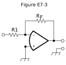
Figure E7-3 - A. 0.21
- B. 4700
- C. 47
- D. 24
Show answer
C. 47
Figure E7-3 is an inverting amplifier, whose voltage gain is RF / R1. With RF = 470 ohms and R1 = 10 ohms, the gain is 470 / 10 = 47 (with the output inverted).
- A. 0.21 does not follow from the resistor values; even the inverted ratio R1 / RF is about 0.021, and this circuit has a gain much greater than 1.
- B. 4700 is RF multiplied by R1; the gain is the ratio RF / R1, not the product.
- D. 24 is about half the correct gain; RF / R1 = 470 / 10 = 47.
E7G08
How does the gain of an ideal operational amplifier vary with frequency?
- A. It increases linearly with increasing frequency
- B. It decreases linearly with increasing frequency
- C. It decreases logarithmically with increasing frequency
- D. It does not vary with frequency
Show answer
D. It does not vary with frequency
An ideal operational amplifier is defined to have infinite gain and unlimited bandwidth, so its gain is the same at every frequency. Real op-amps lose open-loop gain as frequency rises, which is why their gain-bandwidth is specified.
- A. No op-amp, ideal or real, gains more as frequency rises.
- B. Gain that falls with frequency describes real op-amps, not the ideal op-amp, whose bandwidth is unlimited.
- C. A logarithmic decrease is not the behavior of the ideal op-amp, whose gain is constant at all frequencies.
E7G09
What will be the output voltage of the circuit shown in Figure E7-3 if R1 is 1,000 ohms, RF is 10,000 ohms, and 0.23 volts DC is applied to the input?
Figure E7-3 - A. 0.23 volts
- B. 2.3 volts
- C. -0.23 volts
- D. -2.3 volts
Show answer
D. -2.3 volts
For the inverting amplifier in Figure E7-3, Vout = -(RF / R1) x Vin. Here Vout = -(10,000 / 1,000) x 0.23 V = -10 x 0.23 V = -2.3 volts; the output is negative because the signal drives the inverting input.
- A. 0.23 volts would mean a gain of 1 with no inversion; the gain here is 10 and the output is inverted.
- B. 2.3 volts has the right magnitude but ignores the inversion; the signal drives the inverting input, so the output is negative.
- C. -0.23 volts includes the inversion but uses a gain of 1 instead of RF / R1 = 10.
E7G10
What absolute voltage gain can be expected from the circuit in Figure E7-3 when R1 is 1,800 ohms and RF is 68 kilohms?
Figure E7-3 - A. 1
- B. 0.03
- C. 38
- D. 76
Show answer
C. 38
The absolute voltage gain of the inverting amplifier in Figure E7-3 is RF / R1. With RF = 68 kilohms and R1 = 1,800 ohms, 68,000 / 1,800 = 37.8, which rounds to 38.
- A. A gain of 1 would require RF to equal R1; here RF is much larger.
- B. 0.03 is the inverted ratio, R1 / RF = 1,800 / 68,000, about 0.026.
- D. 76 is twice the correct gain of about 38.
E7G11
What absolute voltage gain can be expected from the circuit in Figure E7-3 when R1 is 3,300 ohms and RF is 47 kilohms?
Figure E7-3 - A. 28
- B. 14
- C. 7
- D. 0.07
Show answer
B. 14
The absolute voltage gain of the inverting amplifier in Figure E7-3 is RF / R1. With RF = 47 kilohms and R1 = 3,300 ohms, 47,000 / 3,300 = 14.2, which rounds to 14.
- A. 28 is twice the correct gain of about 14.
- C. 7 is half the correct gain of about 14.
- D. 0.07 is the inverted ratio, R1 / RF = 3,300 / 47,000.
E7G12
What is an operational amplifier?
- A. A high-gain, direct-coupled differential amplifier with very high input impedance and very low output impedance
- B. A digital audio amplifier whose characteristics are determined by components external to the amplifier
- C. An amplifier used to increase the average output of frequency modulated amateur signals to the legal limit
- D. A RF amplifier used in the UHF and microwave regions
Show answer
A. A high-gain, direct-coupled differential amplifier with very high input impedance and very low output impedance
An operational amplifier is a high-gain, direct-coupled differential amplifier (it amplifies signals down to DC) with very high input impedance and very low output impedance. Its behavior in a circuit, such as gain and frequency response, is set by external feedback components.
- B. An op-amp is an analog amplifier, not a digital one, even though its characteristics are set by external components.
- C. Raising a transmitter's output to the legal limit is the job of an RF power amplifier, not an op-amp.
- D. Op-amps are general-purpose amplifiers used mostly from DC through audio and low radio frequencies, not UHF and microwave RF amplifiers.
E7H Oscillators and signal sources: types of oscillators; synthesizers and phase-locked loops; direct digital synthesizers; stabilizing thermal drift; microphonics; high-accuracy oscillators
E7H01
What are three common oscillator circuits?
- A. Taft, Pierce, and negative feedback
- B. Pierce, Fenner, and Beane
- C. Taft, Hartley, and Pierce
- D. Colpitts, Hartley, and Pierce
Show answer
D. Colpitts, Hartley, and Pierce
The Colpitts, Hartley, and Pierce circuits are three common oscillators. The Colpitts takes its feedback from a capacitive divider, the Hartley from a tapped coil, and the Pierce through a quartz crystal.
- A. Taft is not a common oscillator circuit, and an oscillator needs positive feedback, not negative feedback.
- B. Fenner and Beane are not oscillator circuits; of these three names, only Pierce is.
- C. Taft is not an oscillator circuit; Hartley and Pierce are, but the third common one is the Colpitts.
E7H02
What is a microphonic?
- A. An IC used for amplifying microphone signals
- B. Distortion caused by RF pickup on the microphone cable
- C. Changes in oscillator frequency caused by mechanical vibration
- D. Excess loading of the microphone by an oscillator
Show answer
C. Changes in oscillator frequency caused by mechanical vibration
A microphonic is a change in an oscillator's frequency caused by mechanical vibration or shock. Vibration slightly moves components such as coils and capacitors, changing their values and so modulating the frequency.
- A. An IC that amplifies microphone signals is a microphone preamplifier, not a microphonic.
- B. RF picked up on a microphone cable is RF feedback or interference, not a microphonic.
- D. Loading of a microphone by an oscillator is not a recognized effect; microphonics are frequency changes caused by mechanical vibration.
E7H03
What is a phase-locked loop?
- A. An electronic servo loop consisting of a ratio detector, reactance modulator, and voltage-controlled oscillator
- B. An electronic circuit also known as a monostable multivibrator
- C. An electronic servo loop consisting of a phase detector, a low-pass filter, a voltage-controlled oscillator, and a stable reference oscillator
- D. An electronic circuit consisting of a precision push-pull amplifier with a differential phase input
Show answer
C. An electronic servo loop consisting of a phase detector, a low-pass filter, a voltage-controlled oscillator, and a stable reference oscillator
A phase-locked loop is a servo loop: a phase detector compares the output of a voltage-controlled oscillator (VCO) with a stable reference oscillator, a low-pass loop filter smooths the resulting error voltage, and that voltage steers the VCO until it locks in phase with the reference.
- A. A ratio detector is an FM demodulator and a reactance modulator produces FM or PM; neither is part of a basic phase-locked loop.
- B. A monostable multivibrator is a one-shot timing circuit, not a phase-locked loop.
- D. A push-pull amplifier is not a control loop and contains no phase detector or VCO.
E7H04
How is positive feedback supplied in a Colpitts oscillator?
- A. Through a tapped coil
- B. Through link coupling
- C. Through a capacitive divider
- D. Through a neutralizing capacitor
Show answer
C. Through a capacitive divider
A Colpitts oscillator takes its feedback from a capacitive divider: two capacitors in series across the tuned circuit. The connection between them returns part of the output to the input in the right phase to sustain oscillation.
- A. Feedback through a tapped coil identifies the Hartley oscillator.
- B. Link coupling transfers energy between circuits through a small coupling winding; it does not define the Colpitts oscillator.
- D. A neutralizing capacitor cancels feedback in amplifiers to prevent oscillation, the opposite of what an oscillator needs.
E7H05
How is positive feedback supplied in a Pierce oscillator?
- A. Through a tapped coil
- B. Through link coupling
- C. Through a neutralizing capacitor
- D. Through a quartz crystal
Show answer
D. Through a quartz crystal
In a Pierce oscillator, a quartz crystal is connected in the feedback path between the amplifier's output and input. The crystal passes feedback strongly only near its resonant frequency, so it sets and stabilizes the oscillation frequency.
- A. Feedback through a tapped coil identifies the Hartley oscillator.
- B. Link coupling is a way of transferring energy between circuits, not the feedback method of a Pierce oscillator.
- C. A neutralizing capacitor cancels feedback to prevent oscillation in amplifiers, the opposite of what an oscillator needs.
E7H06
Which of these functions can be performed by a phase-locked loop?
- A. Wide-band AF and RF power amplification
- B. Frequency synthesis and FM demodulation
- C. Photovoltaic conversion and optical coupling
- D. Comparison of two digital input signals and digital pulse counting
Show answer
B. Frequency synthesis and FM demodulation
A PLL with a frequency divider in its loop locks a voltage-controlled oscillator to a multiple of a stable reference, which is frequency synthesis. When locked to an incoming FM signal, its control voltage follows the frequency deviation, so the loop also works as an FM demodulator.
- A. A PLL is a small-signal control loop; it does not amplify AF or RF power.
- C. Photovoltaic conversion is what a solar cell does, and optical coupling is what an optoisolator does.
- D. Comparing digital inputs and counting pulses are jobs for digital comparators and counters, not the purpose of a PLL.
E7H07
How can an oscillator’s microphonic responses be reduced?
- A. Use NP0 capacitors
- B. Reduce noise on the oscillator’s power supply
- C. Increase the gain
- D. Mechanically isolate the oscillator circuitry from its enclosure
Show answer
D. Mechanically isolate the oscillator circuitry from its enclosure
Microphonics come from mechanical vibration reaching the oscillator's components. Mechanically isolating the oscillator circuitry from its enclosure, for example with shock-absorbing mounts, keeps vibration from shifting the frequency.
- A. NP0 capacitors have a temperature coefficient near zero, which reduces thermal drift, not sensitivity to vibration.
- B. Reducing power supply noise lowers noise modulation of the oscillator but does not stop the effects of mechanical vibration.
- C. Increasing gain does not reduce microphonics and can make an oscillator less stable.
E7H08
Which of the following components can be used to reduce thermal drift in crystal oscillators?
- A. NP0 capacitors
- B. Toroidal inductors
- C. Wirewound resistors
- D. Non-inductive resistors
Show answer
A. NP0 capacitors
NP0 (also called C0G) capacitors have a temperature coefficient close to zero, so their capacitance barely changes with temperature. Using them in the frequency-determining parts of an oscillator reduces thermal drift.
- B. Toroidal inductors are chosen for self-shielding and compact size; they do not reduce temperature-related frequency drift.
- C. Wirewound resistors have inductance and are not used to reduce oscillator thermal drift.
- D. Non-inductive resistors avoid stray inductance, but resistors are not the frequency-setting parts whose temperature behavior causes drift.
E7H09
What type of frequency synthesizer circuit uses a phase accumulator, lookup table, digital-to-analog converter, and a low-pass anti-alias filter?
- A. A direct digital synthesizer
- B. A hybrid synthesizer
- C. A phase-locked loop synthesizer
- D. A direct conversion synthesizer
Show answer
A. A direct digital synthesizer
A direct digital synthesizer adds a frequency-setting number to a phase accumulator on each clock cycle, uses the resulting phase to look up waveform amplitudes in a table, converts those values to a voltage with a digital-to-analog converter, and smooths the result with a low-pass anti-alias filter.
- B. A hybrid synthesizer combines techniques, such as a DDS with a PLL; the parts listed describe a DDS by itself.
- C. A phase-locked loop synthesizer uses a VCO, phase detector, loop filter, and dividers, not a phase accumulator and lookup table.
- D. Direct conversion describes a receiver that converts RF directly to audio, not a type of synthesizer.
E7H10
What information is contained in the lookup table of a direct digital synthesizer (DDS)?
- A. The phase relationship between a reference oscillator and the output waveform
- B. Amplitude values that represent the desired waveform
- C. The phase relationship between a voltage-controlled oscillator and the output waveform
- D. Frequently used receiver and transmitter frequencies
Show answer
B. Amplitude values that represent the desired waveform
In a DDS, the phase accumulator steps through phase values, and the lookup table converts each phase into the amplitude of the desired waveform at that point, usually a sine wave. The digital-to-analog converter then turns those amplitude values into an analog output.
- A. The lookup table does not store phase relationships to a reference; the phase accumulator tracks phase, and the table converts it to amplitude.
- C. A DDS has no voltage-controlled oscillator; that is part of a phase-locked loop.
- D. Stored operating frequencies are memory channels in a radio's control system, not the contents of a DDS lookup table.
E7H11
What are the major spectral impurity components of direct digital synthesizers?
- A. Broadband noise
- B. Digital conversion noise
- C. Spurious signals at discrete frequencies
- D. Harmonics of the local oscillator
Show answer
C. Spurious signals at discrete frequencies
The main impurities in a DDS output are spurs: unwanted signals at discrete frequencies caused by phase truncation, limited DAC resolution, and DAC nonlinearity. These discrete spurs, more than broadband noise, are what a DDS design and its output filter must deal with.
- A. Broadband noise is present at a low level, but the major DDS impurities are spurs at discrete frequencies.
- B. Conversion errors in a DDS show up mainly as discrete spurious signals rather than as a separate category of noise.
- D. A DDS runs from a reference clock, not a local oscillator, and its characteristic impurities are discrete spurs.
E7H12
Which of the following ensures that a crystal oscillator operates on the frequency specified by the crystal manufacturer?
- A. Provide the crystal with a specified parallel inductance
- B. Provide the crystal with a specified parallel capacitance
- C. Bias the crystal at a specified voltage
- D. Bias the crystal at a specified current
Show answer
B. Provide the crystal with a specified parallel capacitance
A parallel-mode crystal is calibrated to oscillate at its marked frequency when loaded by a specified capacitance, such as 20 pF. Providing that load capacitance in the oscillator circuit puts the crystal on the manufacturer's specified frequency; a different capacitance pulls it slightly off frequency.
- A. Crystals are specified with a load capacitance, not a parallel inductance.
- C. A crystal is a passive resonator and is not biased; its frequency is set by its cut and its load capacitance.
- D. Bias current is not a crystal specification; the operating frequency depends on the load capacitance.
E7H13
Which of the following is a technique for providing highly accurate and stable oscillators needed for microwave transmission and reception?
- A. Use a GPS signal reference
- B. Use a rubidium stabilized reference oscillator
- C. Use a temperature-controlled high Q dielectric resonator
- D. All these choices are correct
Show answer
D. All these choices are correct
Microwave work needs very accurate and stable oscillators, because any reference error is multiplied along with the frequency. A GPS-disciplined reference, a rubidium-stabilized reference, and a temperature-controlled high-Q dielectric resonator are all used to achieve this.
- A. A GPS signal reference is valid, since it disciplines a local oscillator to the satellites' atomic clocks, but it is only one of the techniques listed.
- B. A rubidium-stabilized reference is valid, since it holds frequency to an atomic resonance, but it is only one of the techniques listed.
- C. A temperature-controlled high-Q dielectric resonator is valid, since it provides a stable microwave source directly, but it is only one of the techniques listed.